
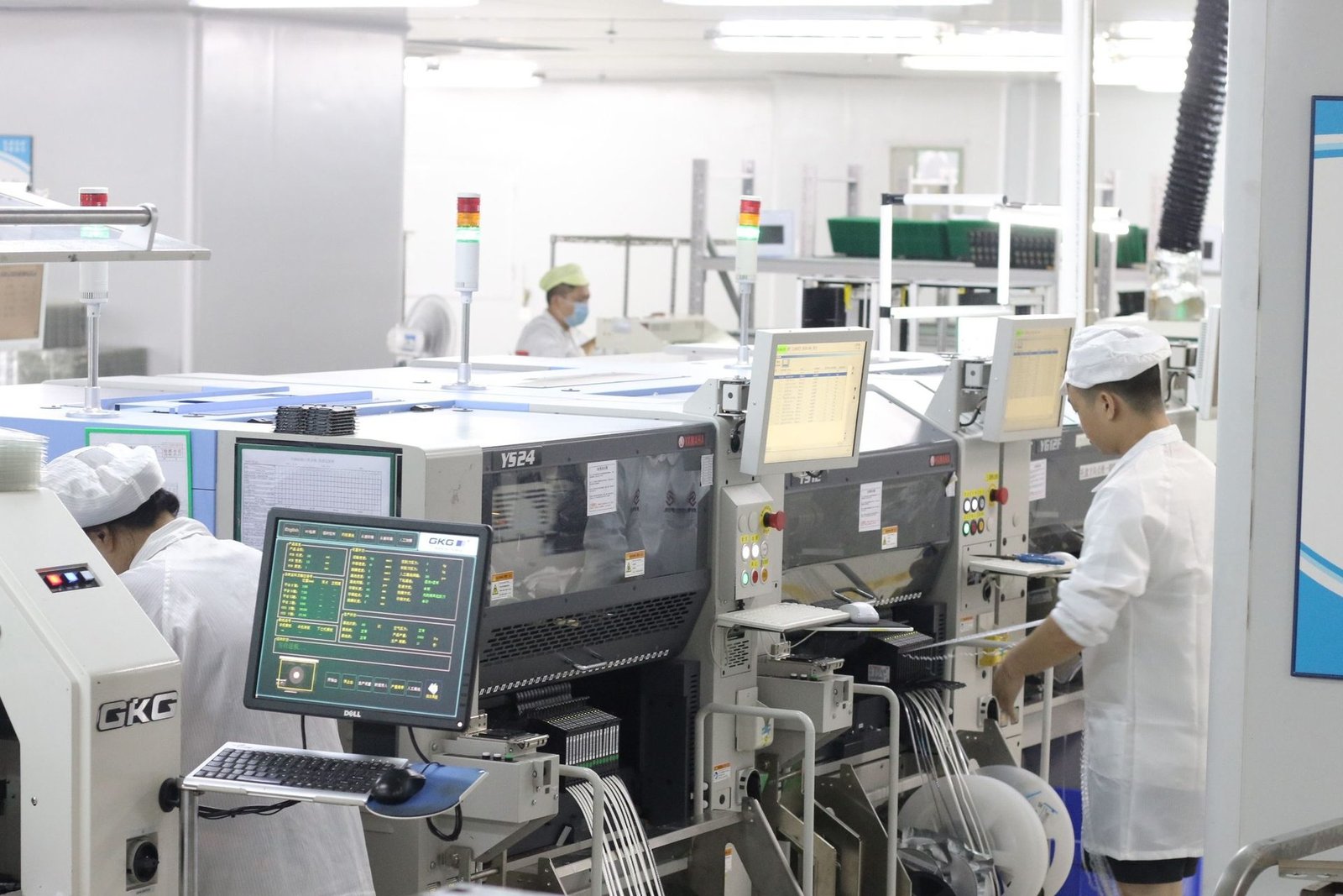
SMT assembly, and the four things your design has to fit
SMT assembly is the part of PCBA a machine does at speed. That makes it cheap per joint and unforgiving about the things a machine cannot fix: how small your parts are, how large your board is, how dense the BGA is, and how many times the board has to go through the oven.
- SMT lines24
- Placement points40.39M a day
- Smallest part01005
- Max board450 × 470 mm
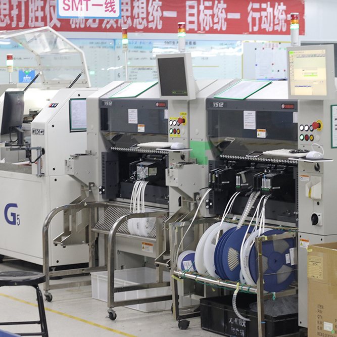
What SMT assembly covers, and what it leaves to through-hole
The two are not competing processes. They solve different problems, and a board that needs both is the normal case rather than the exception.
| Surface-mount (SMT) | Through-hole (DIP) | |
|---|---|---|
| The joint | Sits on the pad, formed by reflowing solder paste — a fillet you can see, but only from above. | Runs through the board and is filled from both sides, usually by wave or by hand. |
| Why you pick it | Small parts, high pin counts, dense routing, anything a person could not place reliably by hand. | Mechanical load: connectors, transformers, relays, terminal blocks, anything a cable pulls on. |
| Where it is weak | Thermal cycling and board flex. A large ceramic capacitor on a board that bends will crack before a through-hole part fails. | Cost and density. Every hole is a drill, a plating step and a placement a machine cannot do at speed. |
| What it costs you | One stencil and one reflow pass per side. | A second operation after reflow, with its own setup and its own inspection. |
| At our plant | 24 SMT lines — 13 YAMAHA, 4 Panasonic, 7 JUKI — at 40.39 million points a day. | 6 DIP lines, with 4 plug-in lines at 800,000 points a day and 3 manual soldering lines at 200,000. |
The usual mistake is treating through-hole as the old process you should design out. On a power board it is often the correct choice: a transformer or a screw terminal that is only surface-mounted will fail at the first cable pull, no matter how good the joint is. If your design is all surface-mount and includes a connector, the question worth asking is what holds the connector against the pull — and the answer is usually through-hole pins.
The four things your design has to fit
Check these before you order. Three are written into the files you send us; the fourth is not in the Gerber file at all, and it is the one that decides how many times the board runs the line.
| Smallest component package | 01005 |
| Largest component package | 2512 |
| BGA pitch | 0.3 mm – 1.25 mm |
| Maximum board size through assembly | 450 mm × 470 mm |
| Minimum order quantity | 1 piece |
1. The smallest package is a decision, not a limit to test
We place 01005, and plenty of boards do not need it. Going one size down costs you at four places at once: the stencil aperture becomes hard to cut cleanly, the paste volume window narrows, the reflow profile has to be tighter, and AOI needs a higher-resolution program. If 0402 fits your layout, 0402 is the cheaper board for exactly the same function. See how package size drives assembly yield.
2. The BGA pitch decides how much of your board is invisible
Down to 0.3 mm, the joints under a BGA cannot be seen by any camera, so the inspection that matters becomes X-ray rather than AOI. That is not a price difference on placement — it is a different inspection programme, and it is priced differently. What each inspection can and cannot see.
3. 450 × 470 mm is the assembly limit, not the fabrication limit
We can fabricate a bare board up to 650 × 1,100 mm. The SMT line takes 450 × 470 mm. A board designed at the fabrication limit is more than three times the area assembly can accept, and it has to be split across a panel before it can run — which changes the tooling, the handling and the price. Decide this before you order boards, not after.
4. One side or two — the only one not in the Gerber file
Every other limit on this list is something we can read off the files you send. Whether the board has parts on both sides is not: the Gerber shows pads on both faces, but not whether you mean us to populate them. It is also the only one of the four that changes the process rather than the machine, so it gets the next section to itself.
Minimum order quantity is one piece, which is not a design limit and so not on this list — but it is not free either: a single board still carries a full stencil, a program, a first-article check and a setup, and none of those divide by quantity. Where the per-unit cost of 100 boards comes from.
Why a double-sided SMT assembly runs the line twice
A board with parts on one side goes through the line once. A board with parts on both sides goes through twice, and the second pass is not a repeat of the first — it is a different problem, because the board now arrives with parts already soldered onto the bottom of it.
On the second pass the board sits on tooling rather than on bare laminate, the parts already placed have to survive another full reflow cycle, and anything heavy enough to fall off on the way through has to be held by adhesive rather than by paste. Those are the three things that change, and each one is decided by your design, not by our line.
- A second stencil. Paste apertures differ between sides because the part mix differs. Two sides means two stencils, and both have to be cut before either can run.
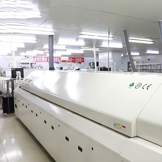
- Two reflow profiles. The second profile has to be low enough not to re-melt the first side into a shift, which narrows the window for the fine-pitch parts on side two.
- Adhesive for the heavy parts. Anything large enough to fall during the second pass is glued down first. That is an extra step, and it is not optional.
- Handling on both faces. Every time the board is turned, a joint is at risk. Double-sided assemblies are also where most handling scrap on a line comes from.
None of that means avoid double-sided. It means if your layout has one large part on the bottom that could have gone on top, moving it is free now and expensive after tooling.
Five SMT defects, and whose decision each one comes from
These five account for most of the scrap on a surface-mount line. Read the last column before you blame the machine — for three of the five, the cause is in the layout or the stencil, not in the placement.
| Defect | What it looks like | What causes it | Whose decision |
|---|---|---|---|
| Tombstoning | A small passive — usually 0402 or smaller — stands up on one end after reflow. | Uneven heating across the part: asymmetric copper on the two pads, paste printed heavier on one end, or the part placed off centre. | Layout and stencil. The placer puts the part where the file says; it cannot fix an unbalanced pad. |
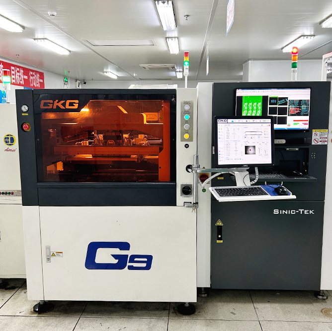
| Bridging | Solder joins two adjacent leads or pads that should be separate. | Too much paste, an aperture that is too large or too close to its neighbour, or paste that has slumped before reflow. | Stencil and print. This is exactly what the 3D SPI runs to catch, immediately after printing. |
| Insufficient solder | A joint forms but carries too little solder to be reliable, or the lead is not wetted at all. | A partially blocked aperture, paste drying in the stencil between prints, a coplanarity problem in the part, or a via beside the pad wicking paste away. | Stencil, part and board design. An unfilled via-in-pad is a common version of this. |
| Wrong or shifted part | The right footprint with the wrong part in it, or the right part slightly off its pads. | Wrong reel loaded, feeder pitch set wrong, or a program offset after a tooling change. | Us. Caught by pre-reflow AOI, one board after it happens — which is why that station exists. |
| Voiding under a thermal pad | X-ray shows a void inside the joint under a QFN or BGA thermal pad, large enough to matter thermally. | Gas from the flux in the paste, a pad pattern that traps it, or a profile that freezes the joint before it can escape. | Paste, profile and pad design together — which is why it is diagnosed by changing one at a time. |
The useful question when a board builds badly is not “how accurate is your machine” — every machine in this class places far more accurately than the paste it is placing the part into — but “which of these five is it, and is that a design problem or a process problem”. Which inspection catches which.
Where SMT yield is decided
Two stations out of the whole line, photographed at our Shenzhen plant. Both of the four limits above are settled here — not at the placement machine, which is the one people watch.
Common questions
Can you do double-sided SMT assembly?
Yes. The board runs the line twice, with a second stencil, a second reflow profile and adhesive under anything heavy enough to fall during the second pass. The practical consequence is cost rather than capability: you pay for two stencils, two setups and two passes. If a large part on the bottom of the board could be moved to the top, moving it costs nothing on paper and real money after tooling.
What is the smallest component you can place?
01005 at the small end and 2512 at the large end, with BGA pitch from 0.3 mm to 1.25 mm. Placing 01005 is a process question rather than a machine question: the stencil aperture, the paste volume window and the AOI resolution all have to be right together. If 0402 fits your layout, 0402 gives you the same function on a cheaper board.
Do you also do through-hole assembly?
Yes. Six DIP lines, four plug-in lines at 800,000 points a day and three manual soldering lines at 200,000 points. Most boards are mixed: surface-mount for the small and dense parts, through-hole for connectors, transformers and anything a cable pulls on. The through-hole operation is a separate step after reflow, with its own setup and its own inspection.
Is there a minimum order quantity for SMT assembly?
One piece. A single board still carries a full stencil, a placement program, a first-article inspection and a line setup, and none of those costs divide by quantity, which is why the per-unit price of a prototype is not the per-unit price of a production run.
Related
Full manufacturing capability
Every parameter in one place: layers, line counts, daily capacity and the two different size limits.
Package size and assembly yield
Why an 01005 board is a stencil problem before it is a placement problem — and where the yield goes.
How a board is tested
SPI, AOI, X-ray and functional test: what each catches, and what each one is blind to.

Send the Gerbers and the BOM
You get back a price and a DFM report — including the parts we think will give you trouble on this line, and the ones you can safely make smaller.