
HDI boards: microvias and build-up
HDI is not a laminate. It is a way of building the board: laser-drilled microvias and build-up layers let a design route more per square millimetre than a mechanically drilled board can. It is what a fine-pitch BGA usually needs.
- Laser holes0.075 mm min
- Layers1 – 32
- Blind/buried viasListed process
- BGA pitch0.3 mm
What HDI actually buys
HDI is not a laminate. It is a way of building the board, and the thing it buys is routing area.
A mechanically drilled hole goes through the whole board, so every layer it passes through loses the routing space around it. A microvia goes only as deep as the layer it has to reach, which frees everything underneath. That is the whole idea: the same footprint routes more signals, or the same routing fits a smaller board — and it is usually what a 0.4 mm-pitch BGA needs before the fan-out closes.
The vias are laser-drilled because a mechanical bit that small breaks. Our limits are 0.075 mm laser-drilled and 0.1 mm mechanically drilled, with blind and buried vias and resin plug holes on the special-process list.
The cost is the build-up. A 1+N+1 board is laminated one extra time; 2+N+2 twice; any-layer more often still. Each cycle is another alignment and another chance of scrap, which is why the stackup — not the layer count — is what a quote is really made of.
HDI and microvia limits
Processing limits are the same as the rest of the plant. The microvia drills are the only number that is specific to this family.
| Minimum laser-drilled hole | 0.075 mm |
| Minimum drill hole diameter | 0.1 mm |
| Layer count | 1 – 32 layers |
| Minimum line width / spacing | 0.06 mm / 0.06 mm |
| Blind and buried vias | On the special-process list |
| Resin plug holes | On the special-process list |
| Blind routing | On the special-process list |
| Impedance control | On the special-process list |
| Maximum board dimensions | 650 mm × 1,100 mm (25.6 in × 43.3 in) |
| Board thickness | 0.2 – 8.0 mm ± 10% |
| Copper weight | 0.5 oz – 12 oz |
| Minimum slot width | 3.0 mm (0.12 in / 120 mil) |
| Surface finish | HASL, ENIG, immersion tin, immersion silver, OSP, ENEPIG, electrolytic hard gold, gold fingers, ENIG + OSP |
| Quality standard | IPC-A-600F / MIL-STD-105D |
| Order quantity | 1 – 500,000 |
| Lead time | Prototype 3–4 days; mass production 8–16 days |
The stackup itself — 1+N+1, 2+N+2 or any-layer — is agreed per design rather than published as a maximum, because it follows from the BGA pitch and the layer count rather than from what the press can close. Send the drawing with both, and the stackup comes back specific to it.
An HDI board is usually a BGA board
The reason to build the microvias is almost always a fine-pitch package, so the assembly side matters as much as the fabrication side.
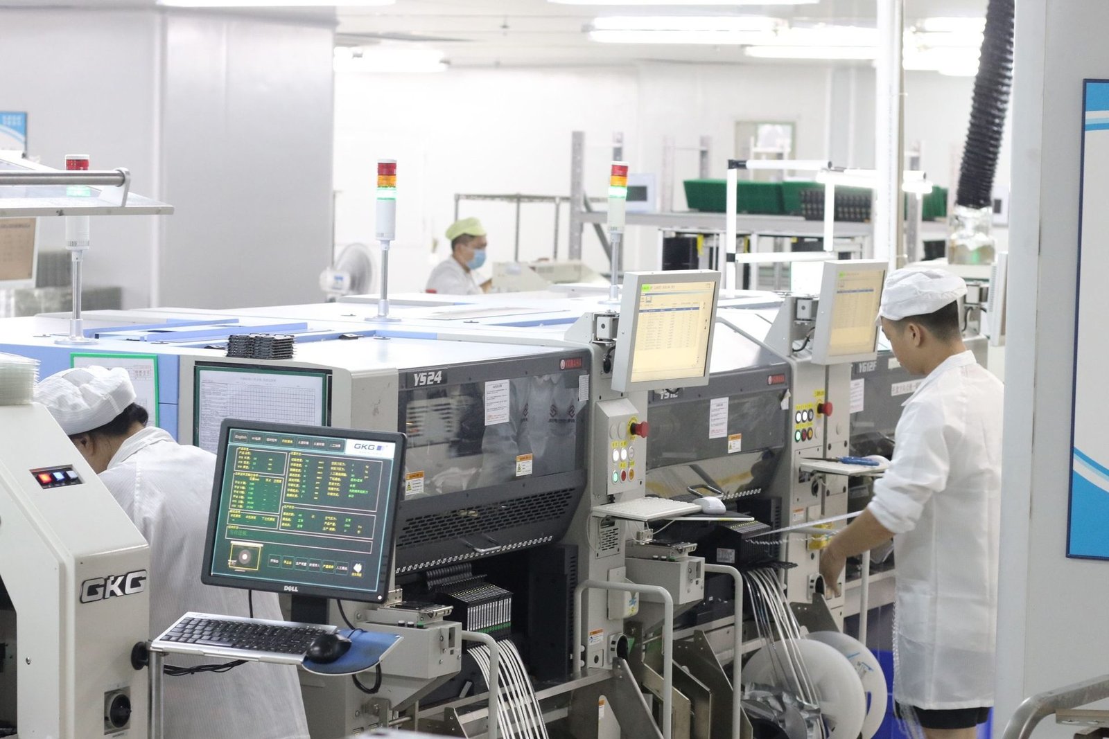
Assembly runs on 24 SMT lines with a placement capacity of 40.39 million points a day, components from 01005 to 2512, BGA pitch down to 0.3 mm, and a board size limit of 450 × 470 mm. A microvia array under a 0.4 mm-pitch BGA is inspected the same way any other hidden joint is — by X-ray rather than by eye, which is what the inspection guide goes through.
The packages themselves — what 01005 and 2512 actually mean, and what each one demands of the line — are in the package guide. HDI is where the small end and the fine-pitch end usually meet.
Where an HDI board fits, and where it does not
HDI is right if…
You want a different family if…
Compare the five board types if the pitch is the only thing pushing you towards HDI — sometimes a better stackup on standard laminate does the same job for less.
Same plant, other families: FR-4 and high-TG rigid · flexible and rigid-flex · aluminium and heavy copper · high-frequency laminates.
Common questions
What is the smallest microvia you can drill?
0.075 millimetres, laser-drilled. Mechanical drilling goes down to 0.1 millimetres.
Do you build blind and buried vias?
Yes. Blind and buried vias, blind routing and resin plug holes are all on our special-process list, alongside half holes, bonding, impedance control, metal cladding, blue glue and carbon ink.
Which HDI stackup can you build?
1+N+1, 2+N+2 and any-layer are all quoted against the drawing rather than against a published maximum, because the stackup follows from the BGA pitch and the layer count. Send both and the answer is specific to your board.
Can an HDI board be assembled here?
Yes. 24 SMT lines, components from 01005 to 2512, BGA pitch down to 0.3 millimetres, and boards up to 450 by 470 millimetres.
How many layers can an HDI board have?
One to 32 in total, counting the build-up layers. What separates an HDI stackup from a standard one is the microvias and the number of lamination cycles, not the layer count.

Microvias are a stackup question
Send the stackup you need with the BGA pitch and the layer count. Which of 1+N+1, 2+N+2 or any-layer the board actually requires comes back with the quote, not before it.